Showing posts with label Power semicoductor diode. Show all posts

Tunnel diode

Definition of tunnel diode:

The tunnel diode is one of the most significant solid state devices which have made their appearance in the last decade. Tunnel diode was invented in the year of 1958 by Leo Esaki. The germanium material is basically used to male tunnel diode. They can also be made from materials as gallium arsenide and silicon materials. The tunnel diode exhibits are also negative resistance in their operating range. therefore it can be used as an amplifier, oscillator and in any switching circuits.

The tunnel diode is heavily doped, highly conductive PN junction diode in which the electric current decreases as the voltage increases. It works on the principle of the method called a tunneling effect. The tunnel diode is used as a very fast switching device in the computer. The tunneling is the phenomenon of conduction in the semiconductor material in which the charge carrier punches the barrier instead of climbing through it. The tunnel diode is a two terminal device with n-type semiconductor called as a cathode and p-type semiconductor called an anode.  It is also used in high-frequency oscillators and amplifier.

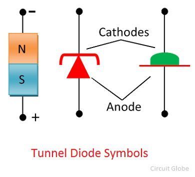
Symbol of tunnel diode:

The symbol of the tunnel diode is shown in the figure given below. It is a two terminal device with p-type semiconductor acting as anode and n-type semiconductor act as a cathode. The n-type semiconductor material emits the electron so it named as the cathode while in p-type material attracts the electrons hence it named as the anode.

Tunnel diode symbol

VI characteristics of tunnel diode:
Forward bias condition:
Under the forward bias condition, the immediate conduction occurs in the diode because of heavily doped conduction happen in the diode. The current in the diode reached the maximum current that diode reached a maximum value of Ip and when the voltage applied is Vp across it. The current value is decreased when more amount of voltage is applied. And it current keep decreasing unit it reaches a minimum value. This minimum value of current is called the method valley current Iv. The tunnel diode and normal PN junction diode characteristics are different from each other.
Reverse bias condition: 
Under the reverse bias condition, the tunnel diode act as a back diode or backward diode. In reverse bias condition, the empty state on the n side aligned with the filled state on the p side. The electron will tunnel through a potential barrier. Because of its high doping concentration tunnel diode acts as an excellent conductor.
Tunnel diode characteristics
The graph above shows that A to point of B the value of current decreases with the increases in voltage. So from figure A to B, the graph shows the negative resistance region of the tunnel diode, This region shows the most important property of the diode. Here in this region, the tunnel diode produces the power instead of absorbing it.
Advantages and disadvantages of Tunnel diode:
Advantages of tunnel diode:
  • Low cost
  • Low noise
  • High speed
  • Fabrication is also very simple
  • Fast response
  • Moderate in operation
  • Low power
  • Longevity
  • Ease of operation
  • Environmental immunity
  • Insensitive to nuclear radiation
Disadvantages of tunnel diode:
  • The voltage range, which can be operated properly in 1 volt or below
  • Being two terminal device, it provides no isolation between output and input circuit
  • The low output voltage swing
  • Tunnel diode cannot be fabricated in a large number
Applications of tunnel diode:
  • Tunnel diode can be used as a switch, oscillator, and  also used in the amplifier
  • It is used as an ultra high-speed switch
  • It shows a fast response
  • It is used as an ultra 
  • It is used as a high-frequency component
  • This diode acts as a logic memory storage device
  • This diode can be used as FM receiver since it is a low current device it is not used more
  • It can be used in modern military equipment
  • This can be used as a microwave oscillator at a frequency of about 10 GHz
  • It is used in nuclear magnetic resource machine
  • It can be used in satellite communication equipment
For detailed information

What is varactor diode

Meaning of varactor diode:

A varactor diode is one kind of semiconductor microwave solid-state device. A varactor diode is a PN junction diode whose capacitance is varied by varying the reverse voltage. These diodes are also named as varicap diodes. A varactor diode is specifically fabricated and optimized such that they permit a high range of changes in capacitance. Before we learn about varactor diode first let us understand the topic of the capacitor.

What is a capacitor?

A capacitor is an electronic component that stores electrical energy or electronic charge in the form of an electric field. The basic capacitor is made up of two parallel conductive plates separated by a dielectric. The two conductive plates act like electrodes and the dielectric act like an insulator. This capacitor, the voltage-dependent device means the output of the diode depends on their input voltage. The varactor diode is used in a place where the variable capacitance is required, and that capacitance with the help of the voltage. This diode also called a volt cap, varicap, voltage variable capacitance or tuning diode. Here first show the figure of the capacitor.


Capacitor symbol

Symbol of varactor diode:


In general, it looks like or similar to that a normal PN junction diode in which one terminal is termed as the cathode and the other terminal is termed as an anode. Here the varactor diode consists of two lines at one end cathode end of normal diode that indicates the capacitor symbol. The one end of a symbol consists of the diode and their other end has two parallel lines.

 varactor diode symbol


Working of varactor diode:

We know that the capacitance of the capacitor is directly proportional to the region of the terminals as the region of the terminals increases the capacitance of capacitor increases when in this mode diode is in the reverse bias mode. The varactor diode is basically made for n-type and p-type of a semiconductor. In n-type semiconductor material the free electrons are the majority carriers while in holes are minority carriers but in p-type of semiconductor holes are the majority carriers and free electrons are the minority carriers. So here when p-type and n-type material are joined together or contact them the PN junction.


This PN junction separates the p-type and n-type semiconductors and the depletion region is created at the PN junction side.  The positive and negative ions make the depletion region. A depletion region is a region where the mobile charge carrier is absent. so diode in reverse bias mode current does not flow. When the diode is connected in forward biasing move the current start flowing through the diode and their depletion region becomes decreases. The depletion region mode does not move from one side to another side. The depletion region blocks free electron from the n-side and hole from the p side region. The depletion-mode region blocks electric current across the PN junction


Depletion region in reverse bias PN junction

Characteristics of the varactor diode

The characteristics of the varactor diode have the following:
  • These diodes are significantly generated less noise compared to other diodes
  • The cost of these diodes is available at lower or more reliable also
  • These diodes are very small in size and very lightweight compared to other diodes
  • There is no use when it is operated in forwarding bias
  • In reverse bias mode, this diode enhanced the capacitance as shown in the graph below

Characteristics of a varactor diode

More detailed information


Advantages and disadvantages of varactor diode:

Advantages of varactor diode:
  • Less noise 
  • The power loss due to noise is low 
  • It is portable due to the small size  
  • Lightweight
  • Reliability
  • It is economical
  • Low cost
  • Small size 
Disadvantages of varactor diode:
  • These diodes are specially designed to work in the reverse biased mode. Hence they are not useful when operating them in the forward bias mode
More detailed information
Read more >> Advantages and disadvantages of a varactor diode


Application of varactor diode:
  • To set LO signal
  • A variable resonant tank LC circuit
  • Electronic application
  • Ultra-high-frequency television sets
  • Harmonic generators
  • Frequency control circuits
  • High-frequency radios
  • Frequency modulator
  • RF phase shifter
  • Frequency multiplier
  • Radio receiver for tunning the circuit
  • Parametric amplifier
  • Bandpass filters
  • Voltage controlled oscillators
More detailed information

Types of diode

The semiconductor diode is a combination of two crystalline semiconductor materials, which designed the two materials know as p-type and n-type. So first let we understand what is n-type and what is p-type of materials

The n-type semiconductor has a larger electron concentration. This is done by introducing a donor as impurities. Here the n-type refers to the negative charge of the electron.

While in p-type of the semiconductor has larger hole concertation, here p-type refers as to the positive charge of the hole.


There are several types of diodes are available for use in electronics design namely a Gunn diode, Laser diode, LED, backward diode, BARITT diode, a PIN diode, PN junction diode, Tunnel diode, Schottky diode, Varactor diode, and Zener diode. Here this article gives the information about what is a diode, what is a Zener diode, different types of Zener diode, application, advantages etc.

The various types of diodes are as follows:

Varactor diode symbol

The symbol of the varactor diode is shown in the figure is given below. The varactor diode symbol consists of with capacitor symbol at the one end of the diode that represents the variable capacitor type characteristics of the varactor diodes to shown in figure.

In general, it looks like or similar to that a normal PN junction diode in which one terminal is termed as the cathode and the other terminal is termed as an anode. Here the varactor diode consists of two lines at one end cathode end of normal diode that indicates the capacitor symbol. The one end of a symbol consists of the diode and their other end has two parallel lines.

Varactor Diode Symbol


Characteristics of varactor diode

The below graph illustrates the relation between the magnitude of reverse bias voltage p-type and n-type layers of a varactor diode, and the magnitude of junction capacitance. They are voltage controlled capacitor and sometimes known as varicap diodes although the word varactor is widely used.

Variable capacitance effect is shown by a normal diode, but the varactor diode is preferred for providing required capacitance changes. The diodes are uniquely optimized and also manufactured such that they enable high range changes in the capacitance device. A varactor diode is categorized based on the properties of a diode junction.

The characteristics of the varactor diode have the following:
  • These diodes are significantly generated less noise compared to other diodes
  • The cost of these diodes is available at lower or more reliable also
  • These diodes are very small in size and very lightweight compared to other diodes
  • There is no use when it is operated in forwarding bias
  • In reverse bias mode, this diode enhanced the capacitance as shown in the graph below

Characteristics of a varactor diode

tunnel diode symbol

The tunnel diode is a highly doped semiconductor device, that is is highly conductive, heavily doped PN junction diode in which the current induces because of the tunneling. The symbol of a tunnel diode is shown in the figure given below. The n-type material emits the electrons and is named as the cathode while P-type material act as the electrons and hence it called as the anode.


tunnel diode symbol

Characteristics of tunnel diode

Forward bias condition:
Under the forward bias condition, the immediate conduction occurs in the diode because of heavily doped conduction happen in the diode. The current in the diode reached the maximum current that diode reached a maximum value of Ip and when the voltage applied is Vp across it. The current value is decreased when more amount of voltage is applied. And it current keep decreasing unit it reaches a minimum value. This minimum value of current is called as the valley current Iv. The tunnel diode and normal PN junction diode characteristics are different from each other.
Characteristics of the tunnel diode
                                           
Reverse bias condition: 
Under the reverse bias condition, the tunnel diode act as a back diode or backward diode. In reverse bias condition, the empty state on the n side aligned with the filled state on the p side. The electron will tunnel through a potential barrier. Because of its high doping concentration tunnel diode acts as an excellent conductor.

The graph above shows that A to point of B the value of current decreases with the increases in voltage. So from figure A to B, the graph shows the negative resistance region of the tunnel diode, This region shows the most important property of the diode. Here in this region shown in, the tunnel diode produces the power instead of absorbing it.

Varactor diode applications

The applications of the varactor diode are mainly used in involve within RF design arena. It mostly used in frequency modulations or tunning circuit where the value of capacitance determines the output modulations frequency. Some of the applications of the varactor diode are listed below:
  • Automatic frequency controller wherein varactor diode is used to set LO signal
  • It is used in a variable resonant tank LC circuit
  • It is used in the electronic application
  • High-frequency radios
  • Frequency modulator
  • RF phase shifter
  • Frequency multiplier
  • It is used radio receiver for tunning the circuit
  • Parametric amplifier
  • Bandpass filters
  • Voltage controlled oscillators
  • Ultra-high-frequency television sets
  • Harmonic generators
  • Frequency control circuits
  • Voltage control oscillator is widely used in receiving and transmitting circuit in the field of communication
  • It can be used in high-frequency areas like Tv tunning and FM radio operations and frequency modulations

Tunnel diode application

Applications of tunnel diode:
  • Tunnel diode can be used as a switch, oscillator, and amplifier
  • It is used as an ultra-high-speed switch
  • It shows a fast response
  • It is used as an ultra 
  • It is used as a high-frequency component
  • Tunnel diode acts as a logic memory storage device
  • It can be used as FM receiver since it is a low current device it is not used more
  • It can be used in modern military equipment
  • It can be used as a microwave oscillator at a frequency of about 10 GHz
  • It is used in nuclear magnetic resource machine
  • It can be used in satellite communication equipment
Practical application of tunnel diode:
  • The tunnel diode is mostly used as a relaxation oscillator circuit
  • It can be used microwave oscillator, which has the frequency above than 10 GHz
  • It can be used as an amplifier
  • It is used as a whenever high switching is needed mostly in control system because it has a switching time of the nanoseconds or picoseconds
  • It is used in satellite communication types of equipment
  • It is used as a memory storage device
  • It is used in nuclear magnetic resource machine
  • It is also used in the military type of equipment like sonars and radars
  • It has a small inductance, capacitance, and also it has negative resistance for that reason it is used in microwave oscillator and relaxation oscillator

tunnel diode definition

The term tunnel diode also called as Esaki diode, this name comes after Leo saki, It was invented in August 1957 by Leo Esaki, Yuriko, and Takashi Suzuki when they were working at Tokyo Tsushin Kogyo. After in 1973 received the Nobel prize in physics for discovering the electron tunneling effect used in these diodes. A tunnel diode is one type of semiconductor diode that has negative resistance due to the quantum mechanical effect called tunneling. The tunnel diode is a highly conductive, heavily doped PN junction diode in which the electric current decreases as the voltage increases. The tunnel diode is a two terminal device with one n-type of semiconductor cathode and other p-type of semiconductor act as an anode. In tunnel diode electric current is caused by the tunneling effect. The tunneling is the phenomenon of conduction in the semiconductor material in which the charge carrier punches the barrier instead of climbing through i

A tunnel diode is used in high-frequency oscillators, computer, and amplifier. The concentration of the impurity in the normal PN junction diode is about 1 part in 10^8 but in the tunnel diode, the concertation of impurity is about 1 part in 10^3. The diode conducts current both in forward as well as in the reverse direction.
Tunnel diode symbol


Zener diode characteristics

The VI characteristics of Zener diodes shown in the figure given below. This curve shows that when Zener diode if forward bias, it works like a normal diode but when the reverse biased voltage applies across to the Zener diode, the Zener diode breakdown occurs in a different manner.

At Zener breakdown voltage the current stary flowing in the reverse direction, it allows only a small amount of leakage current until the voltage is less than Zener diode
At the certain value of reverse voltage, the reverse current will increase suddenly and sharply. This is an indication that the breakdown has occurred. Breakdown occurs called a Zener breakdown. However, the Zener diode exhibits a controlled breakdown that does damage the device.

This graph shows that Zener breakdown is not exactly vertical shown above which shows that the Zener diode has a resistance. This breakdown voltage of the Zener diode depends on the amount of doped applied. If the diode has heavily doped Zener breakdown occurs at a low reverse voltage, on a different way when the diode is lightly doped breakdown occurs at high reverse voltage. The voltage across Zener is represented by the equation is given below.

V = Vz+IzRz


Zener diode characteristics

What is zener diode

Before we learn about Zener diode first let we understand what is a diode?

The semiconductor diode is a combination of two crystalline semiconductor materials, which designed the two materials know as p-type and n-type. So first let we understand what is n-type and what is p-type of materials

The n-type semiconductor has a larger electron concentration. This is done by introducing a donor as impurities. Here the n-type refers to the negative charge of the electron.

While in p-type of the semiconductor has larger hole concertation, here p-type refers as to the positive charge of the hole.


There are several types of diodes are available for use in electronics design namely a Gunn diode, Laser diode, LED, backward diode, BARITT diode, a PIN diode, PN junction diode, Tunnel diode, Schottky diode, Varactor diode, and Zener diode. Here this article gives the information about what is a diode, what is a Zener diode, different types of Zener diode, application, advantages etc.

What is a Zener diode?

The name of Zener diode was named after American physicist Melvin Zener who discovered the Zener effect. The Zener diode is widely used in all kind of electronic circuit equipment.

The Zener diode is a unique diode which allows the current to flow in one direction like a regular diode but is also permits it to flow in the opposite direction. It allows the flow in the opposite direction when the voltage is above a certain value as Zener voltage. Zener diode consists of a highly doped reversed biased, p-n junction diode while operating in the breakdown region.

In a normal diode, the breakdown voltage is very high and also the diode gets damaged totally if a voltage is above the breakdown diode is applied, but in Zener diodes, the breakdown voltage is not like too much high and does not lead to permanent damage of the Zener diode if the voltage is applied.

A Zener diode is a basically P-N junction type of semiconductor diode, which device designed to operate in the reverse breakdown region.  The Zener diode is always connected in reverse direction because it is specially designed to work in reverse direction. The breakdown voltage of the Zener diode is carefully set by controlling the doping level during manufacture.

The symbolic representation of the Zener diode is given below:
Zenor diode
Zener Diode

Zener diode characteristics of Zener diode:


The VI characteristics of Zener diodes shown in the figure given below. This curve shows that when Zener diode if forward bias, it works like a normal diode but when the reverse biased voltage applies across to the Zener diode, the Zener diode breakdown occurs in a different manner.

At Zener breakdown voltage the current stary flowing in the reverse direction, it allows only a small amount of leakage current until the voltage is less than Zener diode

At the certain value of reverse voltage, the reverse current will increase suddenly and sharply. This is an indication that the breakdown has occurred. Breakdown occurs called a Zener breakdown. However, the Zener diode exhibits a controlled breakdown that does damage the device.
Zener diode characteristics
For detailed information: >> Read more

Different types of Zener diodes:
  • Normal diode 
  • Power dissipation
  • Forward voltage
  • Packing voltage
  • Forward drive current
  • Maximum reverse current
For detailed information: >>> Read more

Advantages of Zener diode:
  • High accuracy
  • Small size
  • Power dissipation capacity is very high
  • Low cost
Application of Zener diode:
  • Voltage regulation
  • Voltage reference
  • Switching operation
  • Clamping circuit
  • Various protection circuit
  • Waveform clipper
  • Voltage shifter
  • Voltage stabilizer
  • For meter protection
  • For wave shaping
  • As voltage stabilizer
For detailed information: >>> Read more

Conclusion:
  • We all know that learn about the above topic we understand that this ordinary diode only that it has been doped to have a sharp breakdown voltage.
  • the diode maintains a stable output voltage irrespective of the input voltage provided the maximum Zener current is not exceeded.
  • The Zener diode default operational state is in the breakdown region that we seen above. It means it actually starts to work when the applied voltage is higher than the Zener voltage is in reversed biased.
  • When Zener diode is forward bias, the Zener diode behaves exactly like the normal silicone diode. It conducts with the same 0.7 V voltage drop that accompanies the use of the normal diode.
  • This diode is mostly used in applications involving, voltage regulations, clipping circuits, and voltage shifters.

Types of Zener diode

There are several types of diodes are available for use in electronics design namely a Gunn diode, Laser diode, LED, backward diode, BARITT diode, a PIN diode, PN junction diode, Tunnel diode, Schottky diode, Varactor diode, and Zener diode. Here this article gives the different types of Zener diode.

Different types of Zener diodes:
  • Normal diode 
  • Power dissipation
  • Forward voltage
  • Packing voltage
  • Forward drive current
  • Maximum reverse current
We have to also explain in details for this diode:
  • Normal diode: The nominal operating voltage of Zener diode is also known as the breakdown voltage of the Zener diode, depending on the application for which type of diode is being to be used, this is often the most important criteria for which Zener diode selection.
  • Maximum Zener current: This refers to the minimum current for the Zener diode start operating in the breakdown region.
  • Power dissipation: This diode represents the maximum amount of power the Zener current can dissipate. Exceeding this power rating leads to an excessive increase in the temperature of the Zener diode which could damage it and also lead to the failure of the things connected to it in a circuit. Thus this factor should be considered when selecting the diode with the user in mind.

Zener diode definition

Definition of Zener diode:

The name of Zener diode was named after the American physicist clearance melvin Zener who discovered the special type of Zener effect. The Zener diode is widely used in all kinds of electronics equipment and mainly used in protecting electronic circuit from overvoltage.

The Zener diode is normal semiconductor type P-N junction diodes operating in reversely biased conditions. The Zener diode is always connected in reverse direction because it is specially designed to work in reverse direction. In other words, the diode which is specially designed for optimizing the breakdown region is known as the Zener diode. The breakdown voltage of the Zener diode is carefully set by controlling the doping level during manufacture.
Zener Diode Symbol
Zener Diode Symbol

Zener diode application

The Zener diode is widely used as a shunt regulator or voltage regulator. When connected in parallel with a variable voltage source so the diodes reverse breakdown voltage. The main application of this type of diodes as a voltage regulator. Over a voltage protector as a voltage reference.
  • The Zener diode is used as voltage reference: In the power supply, a many circuit Zener diode finds as a constant voltage provider or a voltage reference. The only conditions are that the input voltage should be greater than apply Zener voltage and also the series resistor should have a minimum value such that the maximum current flow through the device. 
  • Zener diode as a voltage: In DC circuit Zener diode can be used as a voltage regulator or provide a voltage reference. The main use oZ Zener diode lies in the fact that the voltage Zener diode remains constant for a larger change in current. This makes it possible to use a Zener diode as a constant voltage device or a voltage regulator.
  • Zener diode as a voltage clamper : In a circuit involving AC input source, different from the normal PN diode clamping circuit, a Zener diode can be used The diode can be used to limit the peak of the output voltage to Zener diode at one side and to about 0V at another side of the sinusoidal waveform.

Schottky diode symbol

The schematic symbol of schottky diode is shown in figure given below. In schottky diode, the n types of semiconductor acts as the cathode while metal acts as anode. Schottky diode has a aluminium-silicon junction.

This diode also known as hot carrier diodes, Schottky diode has low reverse recover time as well as low junction capacitance

Symbol of schottky diode :


P-N junction diode symbol

A P-N junction diode is a silicon. The P-N junction is the basic element for semiconductor diodes type. One of the terminals is doped with P- types material as well as the other with N - type of material. 

The schematic symbol of P-N junction diode is made up P-type silicon and N-type silicon semiconductor materials.

Symbol of p-n junction diode :